ECE 457 Multilayer and MEMS Reports
The most memorable course from my University of Alberta experience was easily ECE 457 - Microfabrication and Devices. This course covers many of the techniques used in the fabrication of MEMS and microelectronic devices. The lectures provide detailed descriptions and steps of the processes used in the deposition and etching of layers but the lab is where the course really stands out. There are weekly lab sections throughout the term where students don bunny suits and get the privilege of using the University of Alberta NanoFAB facilities to fabricate their own MEMS and multilayer wafers.
The general process of the two lab projects(MEMS and MultiLayer) was to spend a few lab sections depositing and etching layers on the wafer in NanoFAB, followed by a lab section or two in the characterization lab analyzing the results.
The price of this opportunity -- besides increasingly outrageous tuition -- is that two large reports must be written summarizing the process and detailing results.
Below are the two reports that I wrote. They were a lot of work but completely worth it. They likely aren't super fun to read in detail but they include some nice calculations, photos, charts, and graphics showing the processes used.
MEMS
Fabrication of MEMS, analysis of fabrication techniques and results.
Multilayer:
Fabrication of a number of microelectronic devices(resistors, inductors, capacitors) and analysis of their electrical characteristics.
Bonus Images
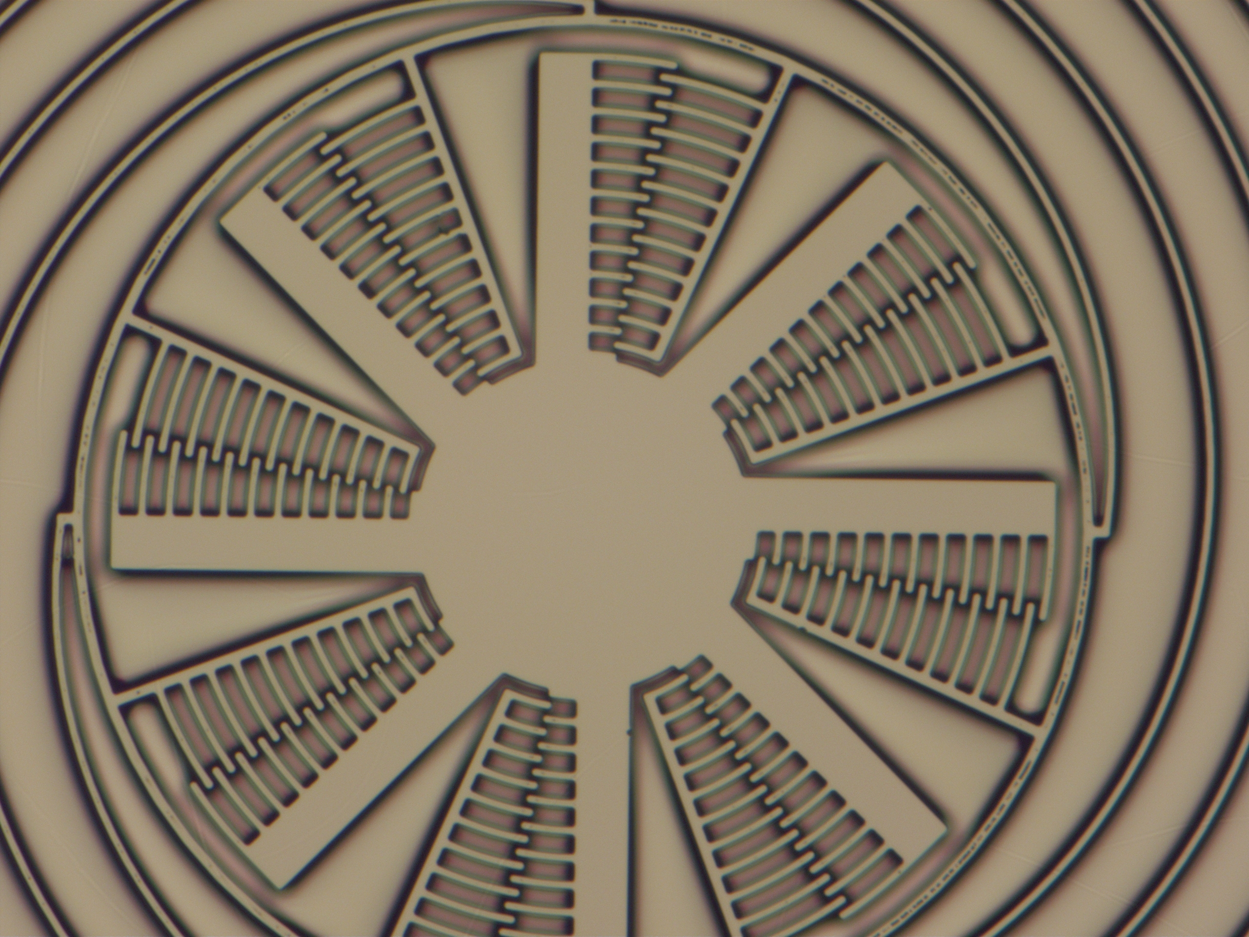
MEMS


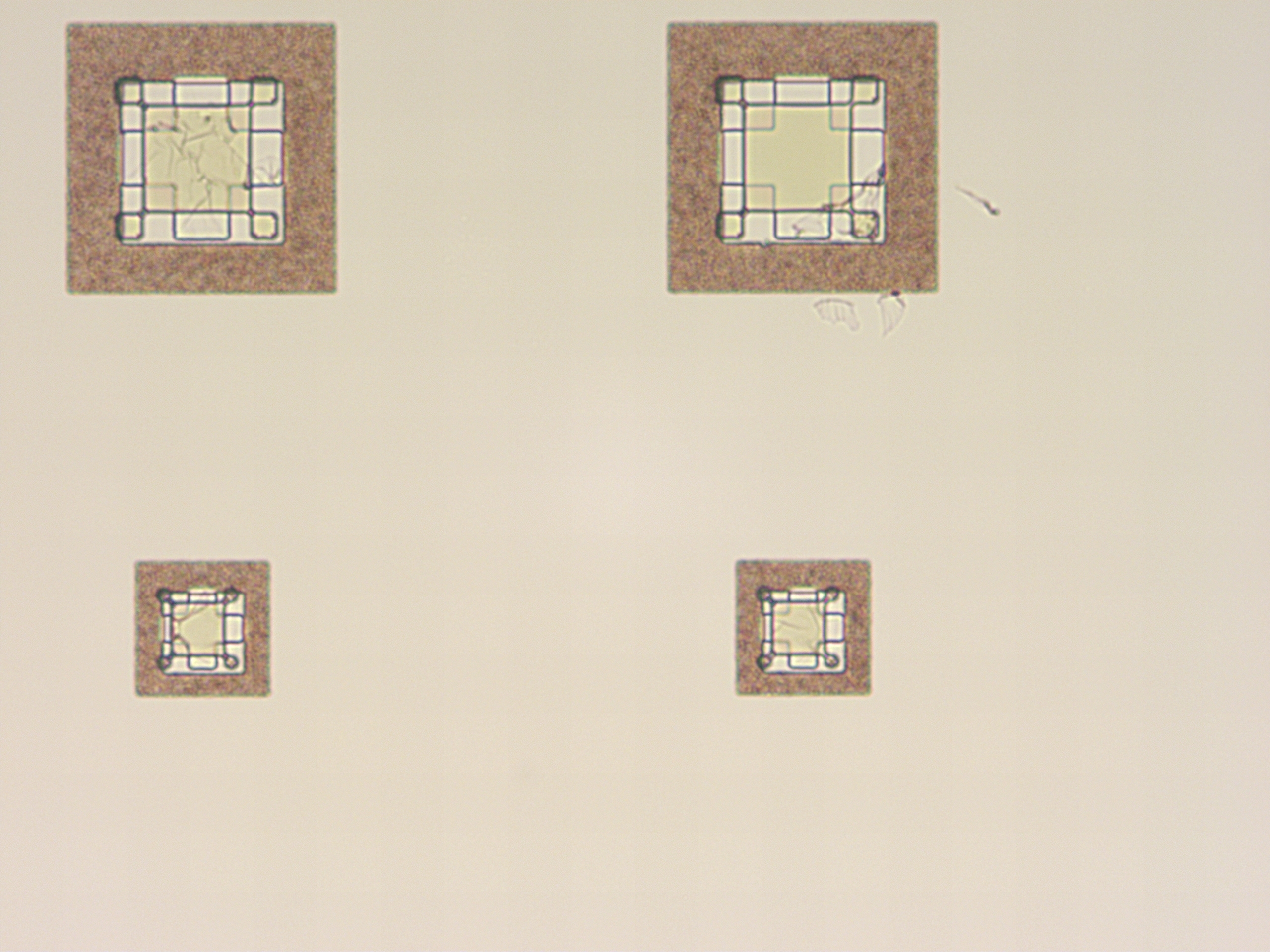
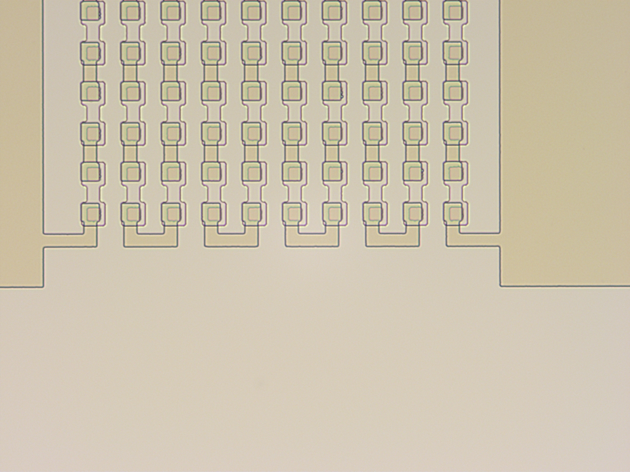
Multilayer


